The 0.6nm Chinese Chip Myth: Deconstructing Mengqi-1000 MoS2 Reality
A viral reel claims China bypassed EUV sanctions to build the world's first 0.6-nanometer commercial chip (Mengqi-1000). Here is the actual semiconductor physics, what the Nature Electronics paper really published, and why 2D materials matter.
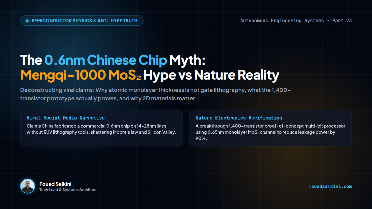
A viral Instagram reel circulating across tech feeds recently proclaimed:
“The West spent years trying to block one machine — the EUV lithography tool — believing it could freeze China’s chip progress. China just walked around it. Meet ‘Mengqi-1000’ — the world’s first 0.6-nanometer chip. Built on 14-to-28-nanometer production lines without EUV… verified in Nature Electronics after 15 years of work by Nanjing University and Huawei.”
With tens of thousands of likes and shares, the narrative suggests that Chinese engineers shattered Moore’s Law overnight, made ASML’s Extreme Ultraviolet (EUV) photolithography scanners obsolete, and developed a sub-nanometer commercial processor ready to power smartphones for a month on a single charge.
As engineers and systems architects, we must separate sensational social media framing from actual solid-state physics.
The paper published in Nature Electronics on May 26, 2026—titled “A bit-parallel molybdenum disulfide computer built through multi-level co-optimization”—is indeed a landmark scientific achievement. But it is not what social media influencers are claiming it to be.
Here is the objective engineering teardown of Mengqi-1000 (梦启-1000).
1. The Core Confusion: Monolayer Thickness vs Gate Lithography
The entire viral premise relies on a fundamental conflation: Material Thickness vs. Transistor Gate Length (Critical Dimension).
What 0.6 nm Actually Refers To:
The “0.6 nanometer” figure describes the physical thickness of a single monolayer of molybdenum disulfide (MoS₂). A single sheet of MoS₂ consists of a plane of molybdenum atoms sandwiched between two planes of sulfur atoms, measuring approximately 0.65 nm in vertical atomic height.
What Commercial Nodes (3nm, 2nm) Refer To:
When TSMC, Intel, or Samsung refer to a “3nm” or “2nm” process node, they are using an industry marketing label corresponding to lateral gate pitches, contacted poly pitches (CPP), and transistor densities exceeding 150 to 250 million transistors per square millimeter.
In Mengqi-1000:
- The channel thickness is 0.65 nm (one atomic layer).
- The actual lateral transistor feature size (gate length and channel dimensions) is hundreds of nanometers, fabricated using standard deep-ultraviolet (DUV) photolithography or standard optical lines (14nm to 28nm and above).
Calling Mengqi-1000 a “0.6nm chip” is equivalent to claiming that a sheet of paper with a drawing of a transistor on it is a “0.1-millimeter transistor” simply because the paper is 0.1 mm thick.
2. Scale of Integration: 1,400 Transistors vs 100+ Billion
To understand where this technology sits on the commercial roadmap, consider the scale:
| Metric | Mengqi-1000 (MoS₂) Prototype | Commercial Silicon (Apple M4 / Nvidia Blackwell) |
|---|---|---|
| Channel Material | 2D Molybdenum Disulfide (MoS₂) | Bulk Silicon / FinFET / GAA Nanosheet |
| Transistor Count | ~1,400 transistors (Multi-bit ALU) | Over 100 to 208 Billion transistors |
| Clock Frequency | Kilohertz / Megahertz range | 3.5 GHz to 4.5 GHz |
| Manufacturing Scale | Laboratory / Cleanroom prototype | Commercial Gigafabs (Hundreds of thousands of wafers/month) |
| Yield & Defect Density | Experimental research yield | Greater than 90% wafer yield for commercial shipment |
Mengqi-1000 is a brilliant multi-bit parallel arithmetic logic unit (ALU). It performs basic binary computing operations across parallel data lines using 2D semiconductors. But it is an exploratory laboratory demonstrator, not a drop-in replacement for desktop CPUs or server GPUs.
3. Why EUV Lithography Still Rules Advanced Silicon
The claim that “China walked around EUV” misunderstands why EUV is indispensable.
EUV photolithography (13.5 nm wavelength) is required to pack billions of transistors tightly together on a silicon die. Without sub-10nm feature printing, interconnect wire delays, capacitance, and sheer die area prevent you from building high-performance modern architectures:
- Interconnect Bottlenecks: A modern GPU requires miles of copper and cobalt interconnects stacked across 15+ metallization layers.
- Die Area Constraints: If you were to build a 50-billion-transistor processor using 28nm optical lines, the silicon die would measure the size of a dinner plate, generate unmanageable heat, and have a wafer yield near zero.
- Lithography Remains Essential: Even if the transistor channel is made of 2D MoS₂, shrinking the gates and interconnects down to commercial density still requires EUV photolithography.
4. The Real Breakthrough: Why Nature Electronics Published It
Stripping away the social media sensationalism does not diminish the true scientific value of the work by Nanjing University, Suzhou National Laboratory, and Huawei. The paper is celebrated because it tackles the greatest crisis facing modern solid-state physics: The Silicon Thinning Wall.
The Quantum Tunneling Limit of Silicon
When silicon channels are made thinner than 3 nm, quantum mechanical phenomena take over:
- Electrons tunnel directly across the source and drain even when the transistor is turned “off” (sub-threshold leakage).
- Surface dangling bonds and lattice roughness scatter carriers, crippling mobility.
The Advantage of 2D Materials (MoS₂)
Unlike 3D bulk crystals like silicon, 2D Transition Metal Dichalcogenides (TMDs) such as MoS₂ possess no out-of-plane dangling bonds. Their surfaces are atomically pristine and chemically saturated.
- Exceptional Electrostatic Gate Control: Because the channel is only one atom thick (0.65 nm), the gate electrode maintains pristine electrostatic control over carrier flow, shutting off leakage almost completely.
- 90% Leakage Power Reduction: Mengqi-1000 demonstrates an extreme reduction in standby leakage current, proving that 2D materials can operate digital logic at drastically lower idle voltages.
- Compatibility with Standard Silicon Lines: The team proved that large-area, wafer-scale MoS₂ films grown by chemical vapor deposition (CVD) can be integrated with standard back-end-of-line (BEOL) silicon processes.
5. Architectural Takeaway & What Comes Next
What is the realistic timeline and engineering trajectory for 2D semiconductors?
    Phase 1: Lab Proof-of-Concept (Current: Mengqi-1000)
    └── ~1,400 transistors, fundamental ALU operations, validation in Nature.
         │
    Phase 2: Hybrid 2D-on-Silicon BEOL Integration (2028-2030)
    └── Monolithic 3D stacking: 2D TMD logic layers atop standard silicon logic for AI cache & sensors.
         │
    Phase 3: Complementary 2D CFETs (2032+)
    └── Replacing silicon completely at the sub-1nm physical gate pitch (requiring High-NA EUV).
The Bottom Line:
- Did China build a 0.6nm commercial chip? No. 0.6nm is the single-atom layer thickness of the MoS₂ crystal, not the transistor’s lithographic feature size.
- Did this eliminate the need for EUV lithography? No. Commercial transistor density and interconnect scaling remain bound to photolithography limits.
- Is this a real scientific milestone? Yes. It demonstrates that atomically thin 2D semiconductors can execute multi-bit parallel computing on standard fabrication lines, providing a vital blueprint for the post-silicon era.
In engineering, physics always trumps marketing. You cannot sanction a country out of physics—and by the same token, you cannot hype your way out of lithography constraints.

Written by Fouad Salkini (فؤاد سلقيني)
General Manager & Tech Lead at Tripnologies and Sync Studios. Systems Architect focusing on AI coding agents, DevOps, and quantitative systems.